Report an Error


AMD Radeon HD 6450
- Graphics Processor
- Caicos
- Cores
- 160
- TMUs
- 8
- ROPs
- 4
- Memory Size
- 512 MB
- Memory Type
- GDDR3
- Bus Width
- 64 bit


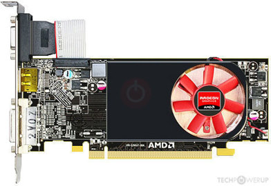
GPU

PCB Front

PCB Back
Recommended Gaming Resolutions:
- 640x480
- 1280x720
- 1366x768
The Radeon HD 6450 was an entry-level graphics card by AMD, launched on April 7th, 2011. Built on the 40 nm process, and based on the Caicos graphics processor, in its Caicos PRO variant, the card supports DirectX 11.2. The Caicos graphics processor is a relatively small chip with a die area of only 67 mm² and 370 million transistors. It features 160 shading units, 8 texture mapping units, and 4 ROPs. AMD has paired 512 MB GDDR3 memory with the Radeon HD 6450, which are connected using a 64-bit memory interface. The GPU is operating at a frequency of 625 MHz, memory is running at 500 MHz.
Being a single-slot card, the AMD Radeon HD 6450 does not require any additional power connector, its power draw is rated at 18 W maximum. Display outputs include: 1x DVI, 1x HDMI 1.3a, 1x VGA. Radeon HD 6450 is connected to the rest of the system using a PCI-Express 2.0 x16 interface. The card measures 168 mm in length, and features a single-slot cooling solution. Its price at launch was 55 US Dollars.
Being a single-slot card, the AMD Radeon HD 6450 does not require any additional power connector, its power draw is rated at 18 W maximum. Display outputs include: 1x DVI, 1x HDMI 1.3a, 1x VGA. Radeon HD 6450 is connected to the rest of the system using a PCI-Express 2.0 x16 interface. The card measures 168 mm in length, and features a single-slot cooling solution. Its price at launch was 55 US Dollars.
Graphics Processor
- GPU Name
- Caicos
- GPU Variant
- Caicos PRO
- Architecture
- TeraScale 2
- Foundry
- TSMC
- Process Size
- 40 nm
- Transistors
- 370 million
- Density
- 5.5M / mm²
- Die Size
- 67 mm²
- Chip Package
- FCBGA-631
Graphics Card
- Release Date
- Apr 7th, 2011
- Generation
-
Northern Islands
(HD 6400)
- Predecessor
- Evergreen
- Successor
- Southern Islands
- Production
- End-of-life
- Launch Price
- 55 USD
- Bus Interface
- PCIe 2.0 x16
- Reviews
- 14 in our database
Relative Performance
Based on TPU review data: "Performance Summary" at 1920x1080, 4K for RTX 3080 and faster.
Clock Speeds
- GPU Clock
- 625 MHz
- Memory Clock
-
500 MHz
1000 Mbps effective
Memory
- Memory Size
- 512 MB
- Memory Type
- GDDR3
- Memory Bus
- 64 bit
- Bandwidth
- 8.000 GB/s
Render Config
- Shading Units
- 160
- TMUs
- 8
- ROPs
- 4
- Compute Units
- 2
- L1 Cache
- 8 KB (per CU)
- L2 Cache
- 128 KB
Theoretical Performance
- Pixel Rate
- 2.500 GPixel/s
- Texture Rate
- 5.000 GTexel/s
- FP32 (float)
- 200.0 GFLOPS
Board Design
- Slot Width
- Single-slot
- Length
- 168 mm
6.6 inches
- TDP
- 18 W
- Suggested PSU
- 200 W
- Outputs
- 1x DVI
1x HDMI 1.3a
1x VGA
- Power Connectors
- None
- Board Number
- 109-C26037-00A
Graphics Features
- DirectX
- 11.2 (11_0)
- OpenGL
- 4.4
- OpenCL
- 1.2
- Vulkan
- N/A
- Shader Model
- 5.0
Caicos GPU Notes
| Generation: Northern Islands Mobile Variant: Seymour Graphics/Compute: GFX4 Display Core Engine: 5.0 Unified Video Decoder: 3.1 Latest Drivers: Windows XP / 8: Catalyst Software Suite 14.4 Windows Vista : Catalyst Software Suite 13.12 Windows 7 / 8.1 / 10: Catalyst Software Suite 15.7.1 / 16.2.1 Beta |
Retail boards based on this design (24)
| Name | GPU Clock | Memory Clock | Other Changes |
|---|---|---|---|
| 750 MHz | 900 MHz | GDDR5 | |
| 650 MHz | 533 MHz | 2 GB, DDR3 | |
| 625 MHz | 600 MHz | 1024 MB, DDR3 | |
| 625 MHz | 600 MHz | 1024 MB | |
| 650 MHz | 600 MHz | 2 GB | |
| 625 MHz | 550 MHz | 1024 MB, DDR3, 183 mm/7.2 inches | |
| 625 MHz | 500 MHz | 1024 MB, DDR3 | |
| 625 MHz | 500 MHz | DDR3, 180 mm/7.1 inches | |
| 625 MHz | 500 MHz | 1024 MB, DDR3, 180 mm/7.1 inches | |
| 625 MHz | 500 MHz | 1024 MB, DDR3, 180 mm/7.1 inches | |
| 625 MHz | 500 MHz | 2 GB, DDR3, 180 mm/7.1 inches | |
| 625 MHz | 500 MHz | 2 GB, DDR3, 180 mm/7.1 inches | |
| 625 MHz | 500 MHz | 1024 MB, DDR3, 180 mm/7.1 inches | |
| 625 MHz | 500 MHz | 2 GB, DDR3, 180 mm/7.1 inches | |
| 625 MHz | 667 MHz | 2 GB, DDR3 | |
| 625 MHz | 800 MHz | 1024 MB, DDR3, 180 mm/7.1 inches, Dual-slot, 2x DVI 1x HDMI | |
| 625 MHz | 800 MHz | 1024 MB, DDR3, 180 mm/7.1 inches, Dual-slot, 2x DVI 1x HDMI | |
| 625 MHz | 800 MHz | GDDR5, 1x DVI 1x DisplayPort 1x VGA | |
| 625 MHz | 667 MHz | 1024 MB, DDR3 | |
| 625 MHz | 667 MHz | 2 GB, DDR3 | |
| 625 MHz | 667 MHz | 146 mm/5.7 inches, 1x DVI 1x VGA 1x S-Video | |
| 750 MHz | 800 MHz | GDDR5, 1x DVI 1x DisplayPort 1x VGA | |
| 625 MHz | 800 MHz | GDDR5 | |
| 625 MHz | 533 MHz | 1024 MB, DDR3, 1x DVI |


Jul 20th, 2025 13:24 EDT
change timezone
Latest GPU Drivers
New Forum Posts
- Technical Issues - TPU Main Site & Forum (2025) (289)
- Windows 11 General Discussion (6158)
- What would you buy? (97)
- Are UPS lithium LiFePO4 batteries finally as cheap as lead-acid? (47)
- Last game you purchased? (869)
- The TPU UK Clubhouse (26559)
- B580 tanks performance with low end CPUs (189)
- What's your latest tech purchase? (24329)
- Disabling MPO (MultiPlane Overlay) in 2025 (46)
- No offense, here are some things that bother me about your understanding of fans. (177)
Popular Reviews
- Razer Blade 16 (2025) Review - Thin, Light, Punchy, and Efficient
- Thermal Grizzly WireView Pro Review
- Pulsar X2 Crazylight Review
- AVerMedia Live Gamer Ultra S (GC553Pro) Review
- MSI GeForce RTX 5060 Gaming OC Review
- SilverStone SETA H2 Review
- Upcoming Hardware Launches 2025 (Updated May 2025)
- Sapphire Radeon RX 9060 XT Pulse OC 16 GB Review - An Excellent Choice
- AMD Ryzen 7 9800X3D Review - The Best Gaming Processor
- NVIDIA GeForce RTX 5050 8 GB Review
TPU on YouTube
Controversial News Posts
- Some Intel Nova Lake CPUs Rumored to Challenge AMD's 3D V-Cache in Desktop Gaming (140)
- AMD Radeon RX 9070 XT Gains 9% Performance at 1440p with Latest Driver, Beats RTX 5070 Ti (131)
- NVIDIA Launches GeForce RTX 5050 for Desktops and Laptops, Starts at $249 (127)
- NVIDIA GeForce RTX 5080 SUPER Could Feature 24 GB Memory, Increased Power Limits (115)
- NVIDIA DLSS Transformer Cuts VRAM Usage by 20% (99)
- AMD Sampling Next-Gen Ryzen Desktop "Medusa Ridge," Sees Incremental IPC Upgrade, New cIOD (97)
- NVIDIA Becomes First Company Ever to Hit $4 Trillion Market-Cap (94)
- Windows 12 Delayed as Microsoft Prepares Windows 11 25H2 Update (92)